Henkel's new products require new packages

Henkel announces that it has worked with STMicroelectronics, one of the world’s largest semiconductor companies and advanced chip packaging technology developers, to validate the performance of Henkel’s Ablestik C100 conductive die attach film materials for production of very small package configurations in a process called ScalPack, which incorporates die with extremely small dimensions
Commercialized in early 2011 following process testing at ST, Henkel’s Ablestik C100 materials – available in 15 micron and 30 micron thicknesses – are now extending the proven advantages of film-based materials to leadframe applications. Notable among the benefits of Ablestik C100 conductive films are the elimination of die tilt, the ability to process thinner die and the facilitation of greater bondline control. Providing a high level of manufacturing latitude, the workability of the new Henkel materials has been established on die sizes ranging from 0.2 mm x 0.2 mm up to 6 mm x 6 mm for multiple package types, including both QFNs and QFPs. These benefits, along with Ablestik C100’s thermal and electrical performance and ability to enable scalable package design, offer a distinct competitive advantage for leadframe packaging specialists.
“Because of the importance of electrical and thermal conductivity, we’ve worked with Henkel to develop a die placement process using its conductive die attach films, as moving to tape-based adhesive materials will guarantee even better workability and in-process control than we currently offer,” says Laura Ceriati, STMicroelectronics Corporate Package Development Director for leaded package platforms. “Our efforts with Henkel will further enable and extend package scalability for the medium-power applications that are a key part of ST’s product portfolio.”
Related news
Related news

Ultrarunner Szilvia Lubics helps with Ultrabalaton
🎧 Hallgasd a cikket: Lejátszás Szünet Folytatás Leállítás Nyelv: Auto…
Read more >
HELL turns 20: Michele Morrone, an exclusive awards ceremony and a spectacular safe await fans at the anniversary event
🎧 Hallgasd a cikket: Lejátszás Szünet Folytatás Leállítás Nyelv: Auto…
Read more >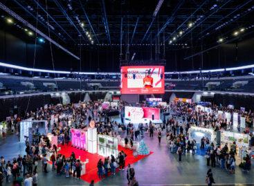
Ticket sales for the 5th Rossmann x Krémmánia Beauty Expo are now open
🎧 Hallgasd a cikket: Lejátszás Szünet Folytatás Leállítás Nyelv: Auto…
Read more >